At MYRESAN, we are proud to be official representatives Central Design Bureau of Machine Building “Donets” (CDBM “Donets”), founded in 1961, more than 60 years of existence, first as the head design bureau of the USSR Ministry of Economic Development and Trade, then as the head design bureau of the Ministry of Industry and Policy of Ukraine in the direction of “Electronic Machine Building”. At present it is engaged in development and manufacture of special technological equipment (STO) for production and processing of functional materials (more than 100 names) of electronic equipment. Over the years, more than 700 types of equipment have been created, including:
– synthesis of semiconductor compounds;
– ingot growing:
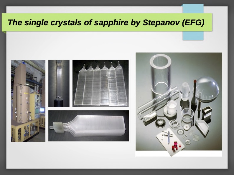
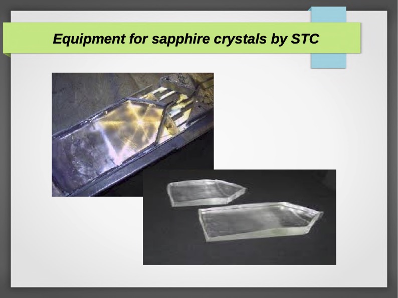
a) bulk and profile single crystals of sapphire;
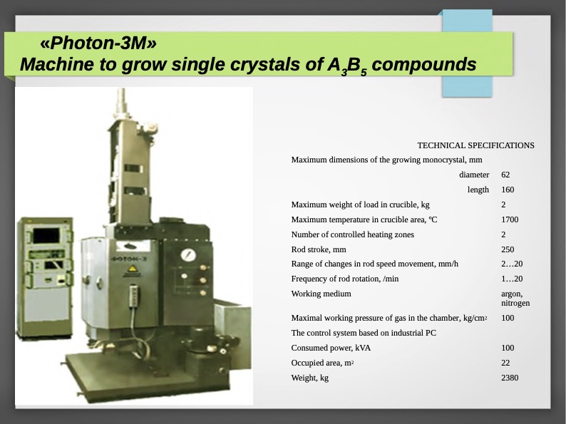
b) A3B5 compounds (gallium arsenide and phosphide, indium phosphide, etc.);
c) А2B6 compounds (zinc selenide and sulfide, cadmium telluride, etc.);
d) ternary compounds (cadmium-mercury-tellurium);
e) ruby;
f) spinel;
g) fianite;
h) oxide compounds (lithium niobate, garnets, langasites, etc.).
– epitaxial growth of layers of semiconductor materials;
– build-up of dielectric and insulating coatings;
– technochemical treatment of wafers and tooling;
– production of quartz products (reactors, crucibles, etc.);
– growing water-soluble large-size single crystals of KDR type;
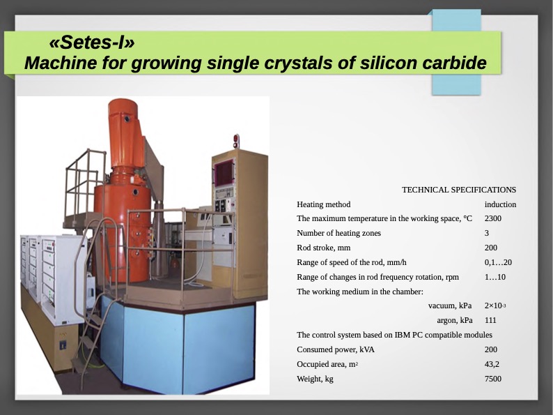
– growing silicon carbide single crystals;
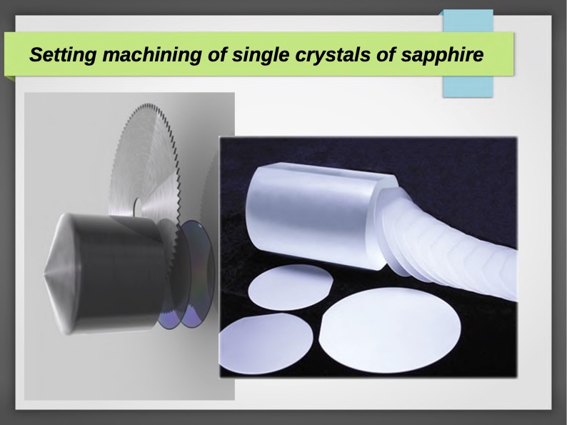
– cutting single crystals into plates, their grinding and polishing;
– oriented cutting of KDR crystals;
– laser thermal treatment of materials, hardening, welding on the basis of CO2 lasers;
– other technological and service equipment.
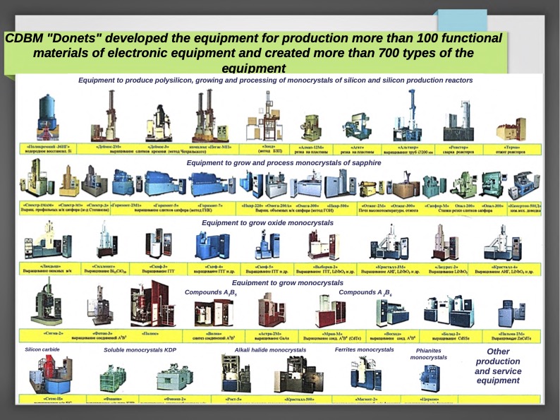
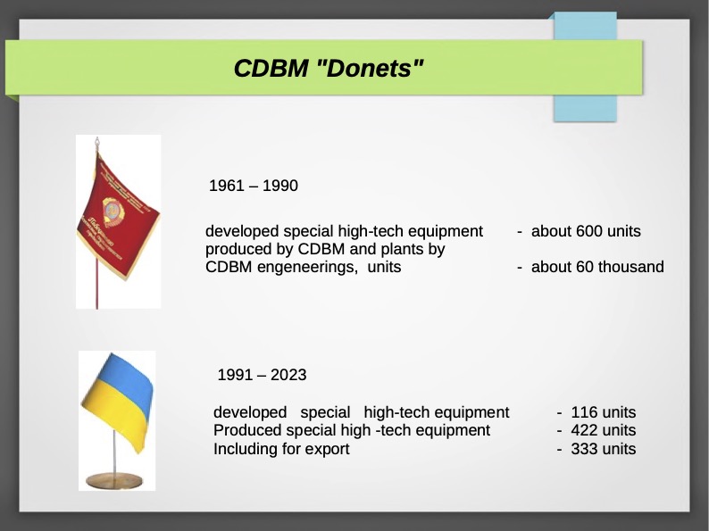
During 1991 ÷ 2014, CDBM “Donets” has developed more than 130 items of new samples of science-intensive special technological equipment of the world level. More than 400 units of equipment were manufactured, which were mainly supplied abroad (Russia, Israel, China, USA, Czech Republic, Switzerland, etc.).
The field of application of the products manufactured on the equipment produced by CDBM “Donets”:
| Sapphire has a unique combination of physical, mechanical and chemical properties: -high radiation and high-energy electron irradiation resistance -stability at high temperatures -very high photo-chemical stability (in particular, under intensive UV irradiation) -chemical stability at temperatures of 540-800 0C – high hardness and wear resistance (hardness is second only to diamond) – high optical transparency in all areas of the spectrum | – CNS substrates for ICs – solid-state laser elements – LEDs on thick substrates, in particular blue LEDs – laser reflectors – high-intensity light sources – solar cell protective coatings. – as a construction material in visible and infrared optics devices – pump lamp shells for high-power lasers – atomic hydrogen source housings – insulators in the production of electron microscopes – engine elements of ultrapure pumps and compressors – chemical ware (crucibles, boats, capillaries, cuvettes, etc.) – thread guides for the textile industry – dies for the glass industry – dental and orthopaedic implants – scalpels for ophthalmology and neurosurgery – as a construction material for working in extreme conditions – insulating substrates for CNS technology – prisms for optical and integrated micrometry receiver systems – strain gauges – input windows for process lasers – reader windows – insulators in the production of electron microscopes – motor elements of ultrapure pumps and compressors – chip substrates – cryogenic heat sinks – laser reflectors – high-intensity light sources – wear-resistant magnetic tape guides and cut-offs – photomultiplier tubes – bearings – pressure chamber windows – laser elements – UV photocathode tube windows – costume jewellery – watch glasses |
| A3B5 compounds Gallium arsenide (GaAs) | – light-emitting diodes – solar cells – lasers – photodetectors – microwave devices – Microdevices (field-effect transistors, multipliers, parametric and avalanche-span diodes, Gan diodes, varactors) |
| Gallium phosphide (GaP) | – SIS (ultrafast integrated circuits) – Hall sensors – light-emitting diodes – photomultipliers – ICs (integrated circuits), SIS (ultrafast integrated circuits) – microwave circuits – electrovacuum devices |
| Indium phosphide (InP) | – vidicon targets – power diodes – solar cells – photodetectors – laser diodes – microwave devices – Gunn diodes |
| A2B6 compounds Zinc selenide (ZnSe), zinc sulphide(ZnS), zinc-cadmium sulphide (Znx Cd1-x S) | – Quantoscopes of blue and blue radiation colours – UV quantoscopes and receivers – electro-optical modulators |
| Cadmium telluride (CdTe), zinc-cadmium telluride (CdZnTe) | – Radiation and IR radiation receivers – optical elements of infrared optical systems |
| Oxide single crystals | Acoustoelectronics |
| Lithium niobate (LiNbO3) Lithium tantalate (LiTaO3) | – high-temperature piezo elements; – delay lines in colour television; – industrial frequency filters Optoelectronics – elements of nonlinear optics; – laser radiation modulators; – frequency multipliers; – parametric oscillators (light generators); – optical frequency generators; – memory elements in volume-phase holography; – electro-optical gates. |
| Aluminium yttrium garnet (Al3Y5O12) | Jewellery – semi-precious stones. Quantum electronics: – Active element in solid-state lasers; – laser localisation and target designators; – night vision devices. Medicine: – Surgery (scalpel); – ophthalmology (retinal detachment, glaucoma, vascular tumours); – laser acupuncture; – laser therapy (removal of age spots, tattoos). |
| Gadolinium gallium garnet (Gd3Ga5O12) | Agriculture: – laser irradiation of grain (increasing yields); – pruning of grape bunches. – non-magnetic substrates for epitaxial layers of multi-component ferrites used as an active medium in domain processes. – memory devices; – logic and switching devices; – information display devices and systems; -a new class of domain devices on CMD lattices, which can simultaneously fulfil the functions of storage devices and logic elements. -when doped with neodymium (Nd) can be used as an active body in lasers. |
| Bismuth silicate (Bi12SiO20) | Acoustoelectronics – Low-cost small-size SAW (surface acoustic wave) devices – low-frequency filters for long-distance communication systems (phased antenna arrays) – Radiolocation, communications, radio and television Medicine – X-ray topography Nuclear physics – nuclear radiation detectors |
| Potassium titanyl phosphate, lithium-niodymium tetraphosphate(LiNdP4O12) | Quantum electronics – miniaturised wavelength-variable solid-state lasers – laser localisation and designators – night vision devices – radiation sources for fibre-optic communication lines |
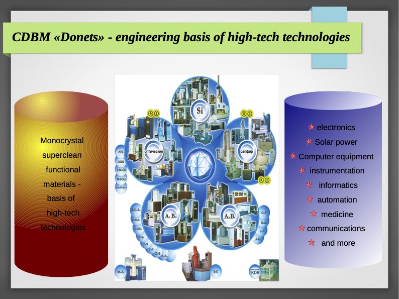
Central Design Bureau of Machine Building “Donets” (CDBM “Donets”) was founded in 1961 and existed for 60 years as head company of the Ministry of Electronic Industry. Currently, it ‘s functioning as part of the National Academy of Sciences of Ukraine, develops and manufactures special technological equipment for production and processing of functional materials (more than 100 types of electronic equipment). Over the years, it created more than 700 types of equipment, including those for: – Synthesis of semiconductor compounds; – Growing of ingots of superclean silicon, monocrystals of electronic silicon and silicon for solar power, volume and profile of single crystals of sapphire, A3B5 compounds (arsenide and gallium phosphide, indium phosphide, and others). Compounds A2B6 (selenide and zinc sulfide, cadmium telluride and others), ternary compounds (cadmium-mercury- tellurium), ruby, spinel, fianites, oxide compounds (lithiumniobate, grenades, langasiteetc.).- Epitaxial growth of layers of semiconductor materials;
– Growth of the dielectric and insulating coating;
– Technical-chemical wafer processing and tooling;
– Production of products of quartz (reactors, crucibles, etc.).
– Growth of large single crystals of water-soluble type of CRA;
– Growth of single crystals of silicon carbide and application of chemically pure siliconcarbide on products;
– Cutting of single crystals on plates, their grinding and polishing;
– Cutting-oriented crystals CRA;
– Laser thermal processing of materials, hardening, welding, based on CO2 lasers;
– Other technolological and service equipment.
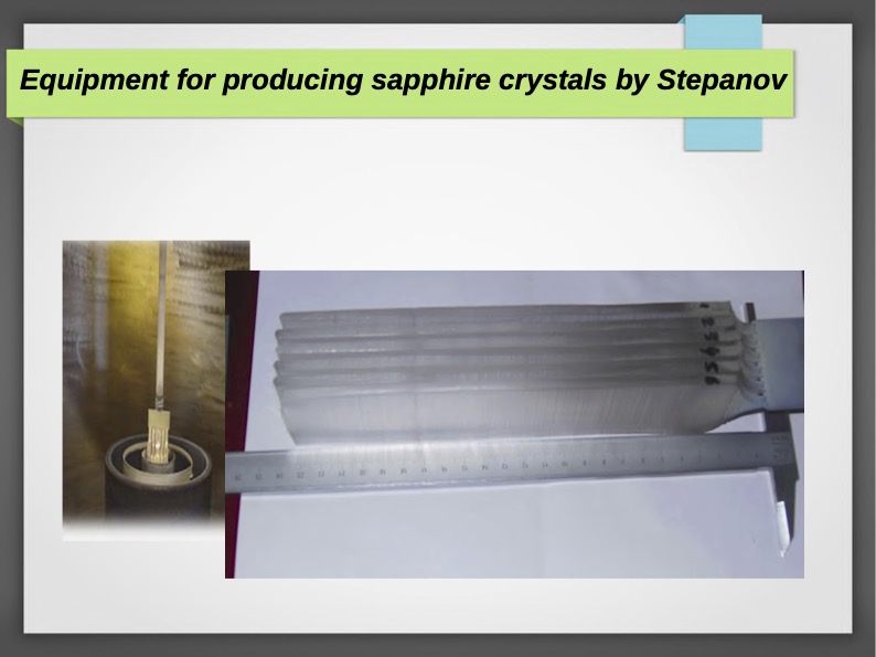
During the 1991÷2023 CDBM “Donets” developed more than 130 kinds of new models of high-tech equipment of high standard quality and produced more than 400 units of equipment, which are mainly exported abroad (Israel, China, Russia, USA, Czech Republic, Switzerland and others). In recent years, CDBM “Donets” created a wide range of equipment for large-sized single crystals of sapphire by the GOI, STC, Stepanova and their mechanical processing:
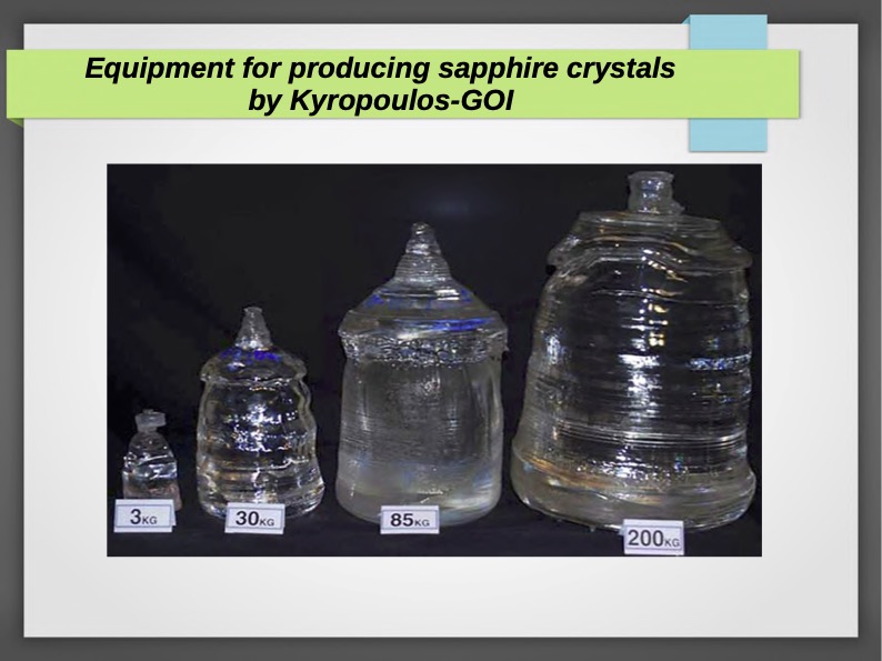
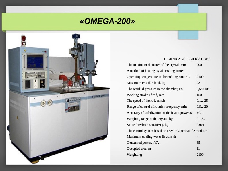
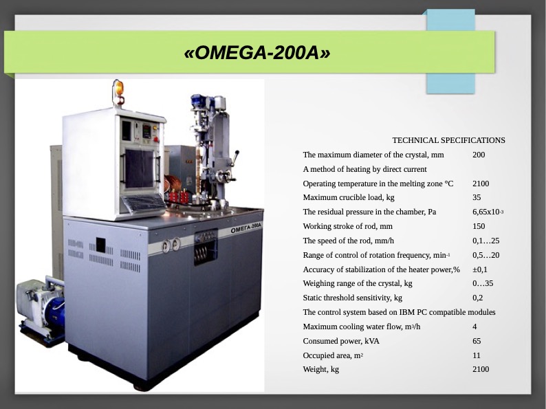
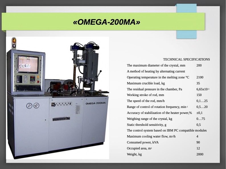
– machine type “Omega”, “Icar,” – to grow single crystals of sapphire by Kyropoulos-GOI method;
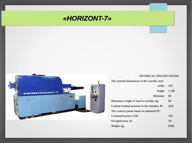
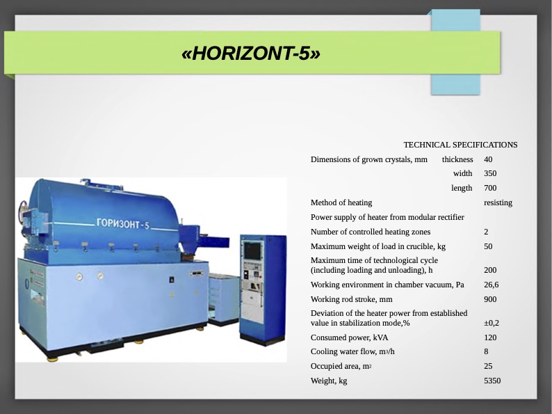
– machine type “Horizont” – for growing large single crystals of sapphire by STC;
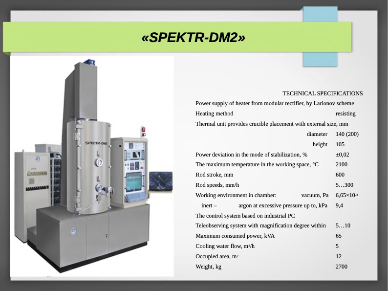
– machine type “Spectr” – for growing shaped single crystals of sapphire;
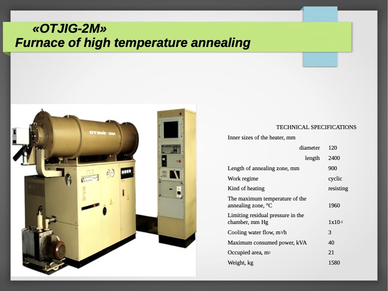
– machine type “Otjig” – for high temperature annealing of single crystals of sapphire;
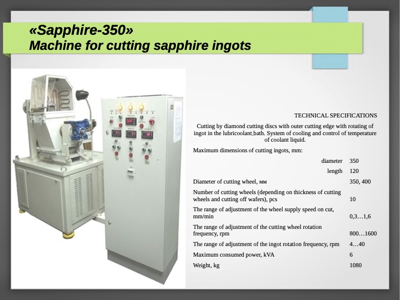
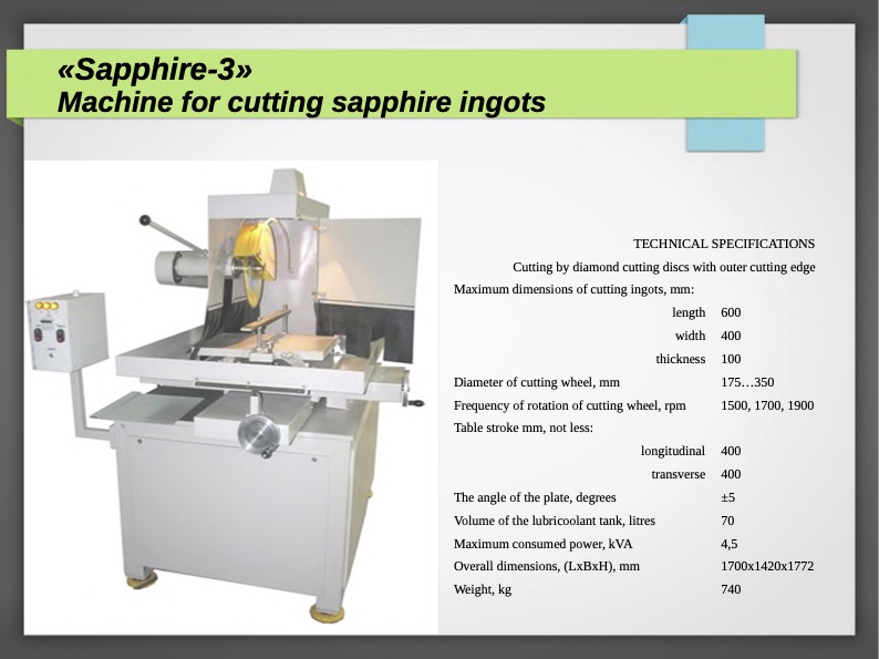
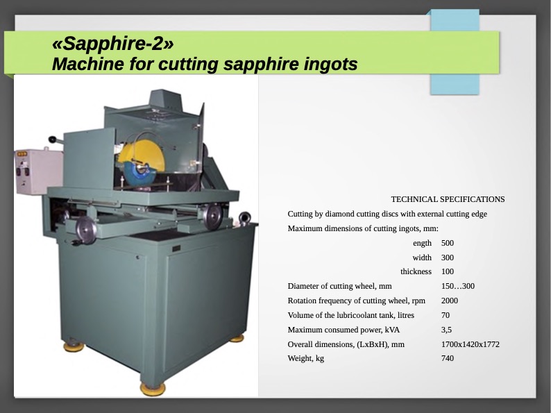
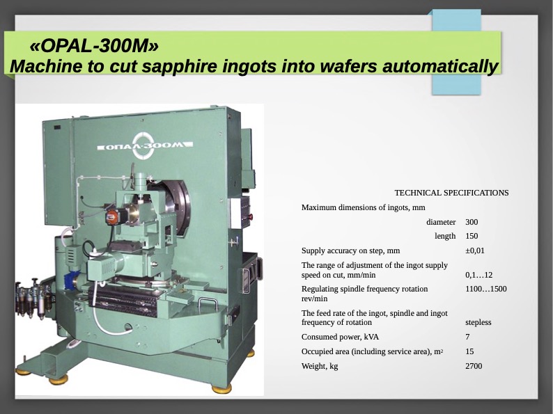
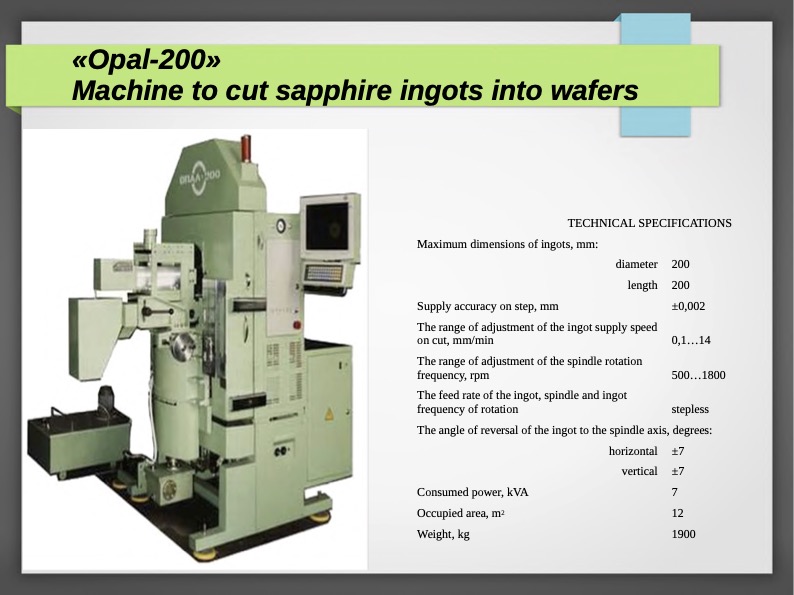
– cutting machine “Opal” “Opal-M”, “Opal-200”, “Opal-300”, “Sapphire”, “Sapphire-M”, “Sapphire-3”,
“Opal-300M” – for cutting monocrystalline sapphire ingots up to 300 mm in diameter;
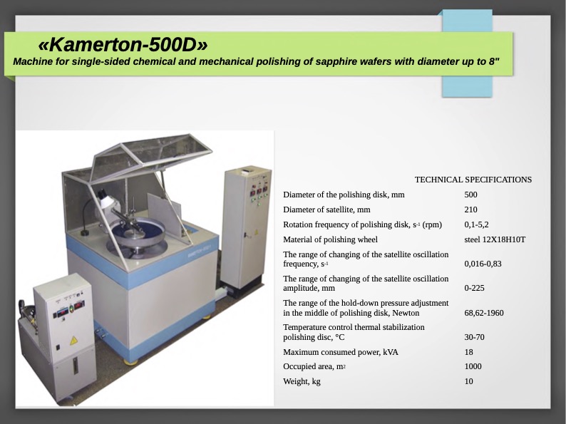
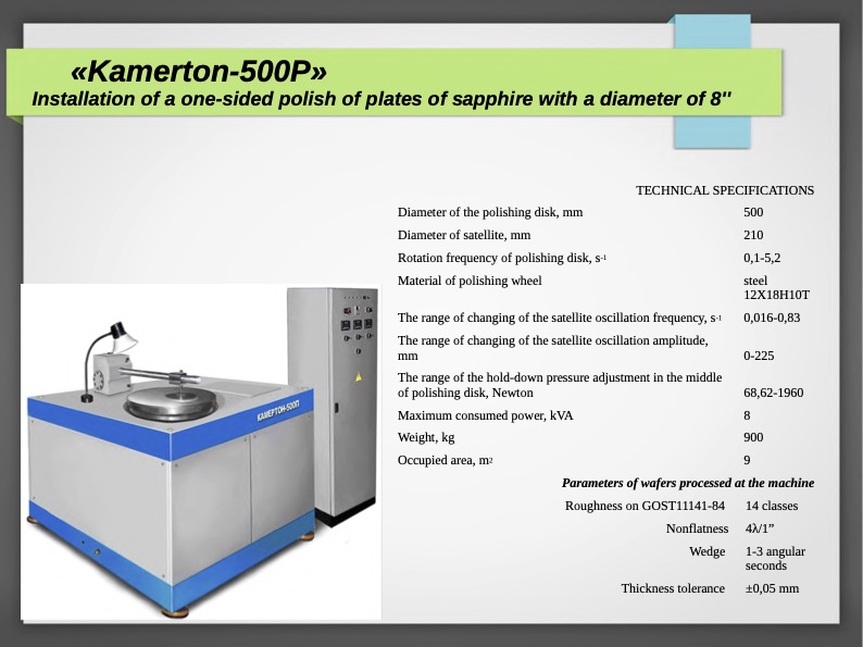
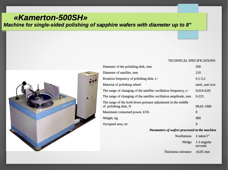
– machine type “tuning fork” – for grinding, polishing, chemical-dynamic polishing of sapphire wafers.
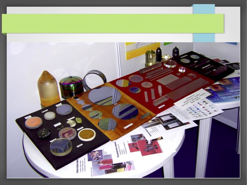
Sapphire
Sapphire, due to the unique characteristics:
– High hardness and wear resistance;
– Stability at high temperatures;
– The chemical resistance in different environments;
– High optical transparency in all regions of the spectrum;
– Very high photochemical stability;
– High radiation resistance, is increasingly used in all areas of human activity: in cosmic and defense technology, chemistry, medicine, textiles and electronics as substrates for high-brightness light-emitting diodes and integrated circuits, instrumentation, lighting, automotive, as a construction material, in laser technology for the manufacture of watch glasses, lenses, windows in all kinds of applications, cash registers, etc.